
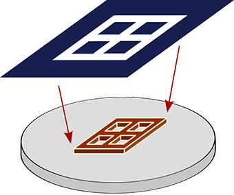
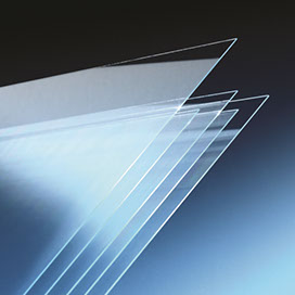
Supttering Targets
Sputtering Targets Applications & Markets
Our versatile product development specialists work with you to meet even the most demanding production parameters in the wide range of applications for sputtering targets.
Material List
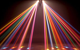
 Sputtering Targets for Displays
Applications
LCD (TFT & Color Filter)
PDP (PDP-Filter)
OLED
Touch Panel
Electronic Paper
Layer-Functions
Transparent high refractive index
Transparent Conductive Oxide (TCO)
Adhesion and barrier
Black Matrix
Electrodes & interconnects (metal & metal alloys)
Standard Materials
Al Aluminium 4N, 5N
Ag Silver 3N7
Ag-alloys Silver alloys 3N7
Au Gold 4N
Cr Chromium 3N7
Cu Copper 4N, 4N7
Mo Molybdenum 3N5
Nb Niobium 3N
NbOx Niobium Oxide 3N5, 4N
Si Silicon 5N
Ta Tantalum 3N5
Ti Titanium 2N7, 3N, 4N5
TiOx Titanium Oxide 3N5, 3N
ZAO® / AZO Zinc Oxide Aluminum Oxide 3N
New Materials
Metal- and ceramic-alloys in various compositions
Tube targets (metals, ceramics, and their alloys) bonded on backing tubes or monolytic
Spraying and casting technology for tube target production
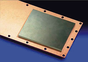
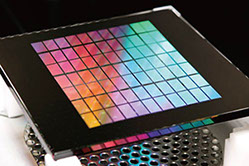 Photo Mask
Applications
Electronic devices - CPU, memories (semiconductor/ IC)
Discreet components with a single task - transistors, memories
Light receiving/ emitting elements - CCD/CMOS image sensors, LED
PWB - motherboards
Display devices - LCD, OLED
MEMS(Micro Electro Mechanical System) - acceleration sensors
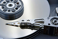
Magnetic heads for hard disks
Heads for inkjet printers
Standard Materials
Cr
Ni
Fe
Ag alloy
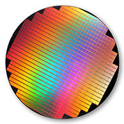 Semiconductor
Applications
IC-Interconnects
Backside-Metallization
Underbump-Metallization
High-K
MEMS
Optoelectronics
Standard Materials
Ag Silver 3N, 4N, 5N
Ag alloys Silver (corrosion resistant) alloys 3N, 4N, 5N
Au Gold 4N, 5N
AuAs alloys Gold Arsenic alloys 4N, 5N
AuGe alloys Gold Germanium alloys 4N, 5N
AuSb alloys Gold Antimon alloys 4N, 5N
AuSn alloys Gold Tin alloys 4N, 5N
Ge Germanium 5N
Ir Iridium 3N
Ni Nickel 3N5
NiFe alloys Nickel Iron alloys 3N
NiPt alloys Nickel Platinum alloys 3N / 4N+
NiTi alloys Nickel Titanium alloys 3N5
NiV alloys Nickel Vanadium alloys 3N5
Pd Palladium 3N5, 4N
Pt Platinum 3N5, 4N
Rh Rhodium 3N
Ru Ruthenium 2N8, 3N, 3N8
Sn Tin 5N
TaAl alloys Tantalum Aluminium alloys 3N5
Ti Titanium 3N, 4N, 4N5, 5N
WTi alloys Tungsten Titanium alloys 4N5
Summit-Tech is a major supplier of sputtering targets and evaporation materials for the semiconductor and electronic industry. As a material specialist, we rely on our extensive know-how in metallurgy and production technologies.
With our product portfolio and specialties, we offer a broad range of target materials for various electronics applications.
Standard Materials
BaSrTiO3,
BiSrTa(Nb)Ox,
Sr2Nb2O7,(Sr,Ba)
Nb2O6,BTO,
STO,
PbTiO3,
PZT,
PLT,
PLZT,
Ir,
Ru,
Ir-Pt,
Ir-Ru,
Pt
Dielectric & Electrode
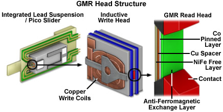
GMR Head
Researchers at IBM soon realized the importance of GMR for hard disk drives and introduced the first GMR read head in 1997. This new type of read head, now widely used, consists of four layers:
a layer of ferromagnetic material (often a nickel-iron alloy) that is closest to the disk and acts as the sensor. It’s called the free layer because the direction of its magnetic field switches to align with the particular bit it happens to be reading at any given moment
a spacer of non-magnetic material (like copper) that serves as a buffer between the two magnetized layers
a pinned layer (often cobalt) that has a fixed, unchanging magnetic orientation
an exchange layer of a material that insulates the pinned layer from outside magnetic fie
Standard Materials
Pure Mn, Mn+a(a:Fe, Ni,Ir, Rh,Ru, Pt, Pd,Cr), NiO, CoO,Fe2O3, Al2O3
Standard Materials
R1-xSrxMnO3(R:La, Nd,Sm, Pr, Gd),
R1-xCaxMnO3
GMR For Laser Ablation
Applications
The simplest application of laser ablation is to remove material from a solid surface in a controlled fashion. Laser machining and particularly laser drilling are examples; pulsed lasers can drill extremely small, deep holes through very hard materials. Very short laser pulses remove material so quickly that the surrounding material absorbs very little heat, so laser drilling can be done on delicate or heat-sensitive materials, including tooth enamel (laser dentistry). Several workers have employed laser ablation and gas condensation to produce nano particles of metal, metal oxides and metal carbides.
Another class of applications uses laser ablation to process the material removed into new forms either not possible or difficult to produce by other means. A recent example is the production of carbon nanotubes.
Standard Materials
CoPt,
CoCrPt,
CoCrTaPt,
CoCrTaPt+SiO2(Al2O3),
NiP series(Foundation film),
Cr, C+a(protection film)
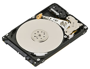
Hard Disks
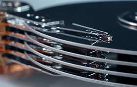
The platters are made from a non-magnetic material, usually aluminium alloy, glass, or ceramic, and are coated with a shallow layer of magnetic material typically 10–20 nm in depth, with an outer layer of carbon for protection. For reference, a standard piece of copy paper is 0.07–0.18 millimetres (70,000–180,000 nm).
Standard Materials
TbFeCo,
GdFeCo,
DyFeCo,
Al-Ti,
Al-Cr,
Al-Ta,
Si-B.
Optical Magnetic Memory
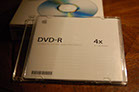
The larger storage capacity of a DVD-R compared to a CD-R is achieved through smaller pit size and smaller track pitch of the groove spiral which guides the laser beam. Consequently, more pits can be written on the same physical sized disc. In order to write smaller pits onto the recording dye layer, a red laser beam with a wavelength of 640 nm (for general use recordable DVD, versus a wavelength of 780 nm for CD-R) is used in conjunction with a higher numerical aperture lens. Because of this shorter wavelength, DVD-R and DVD+R use different dyes from CD-R to properly absorb this wavelength.
DVD-R discs are composed of two 0.6 mm acrylic discs, bonded with an adhesive to each other. One contains the laser guiding groove and is coated with the recording dye and a silver alloy or gold reflector. The other one (for single-sided discs) is an ungrooved 'dummy' disc to assure mechanical stability of the sandwich structure, and compatibility with the compact disc standard geometry which requires a total disc thickness of about 1.2 mm. The sandwich structure also helps protect the data containing layer from scratches with a thick "dummy" disc, a problem with CDs, which lack that structure. Double-sided discs have two grooved, recordable disc sides, and require the user to flip the disc to access the other side. Compared to a CD's 1.2 mm thickness, a DVD's laser beam only has to penetrate 0.6 mm of plastic in order to reach the dye recording layer, which allows the lens to focus the beam to a smaller spot size to write smaller pits.
In a DVD-R, the addressing (the determination of location of the laser beam on the disc) is done with additional pits and lands (called land pre-pits) in the areas between the grooves. The groove on a DVD-R disc has a constant wobble frequency used for motor control, etc.
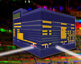
An IBM chip that integrates both electronic and photonic components – a rare example of scaling lasers down small enough to fit on a chip die.
Standard Materials
GeSbTe,
AgInSbTe,
ZnS-SiO2,
Ai-Ti,
Al-Cr,
Al-Ta,
Phase Change of Optical Memory
Basically, the British researchers have taken a chalcogenide glass — which are always p-type semiconductors — and managed to turn it into an n-type semiconductor. (In this case, they germanium telluride (GeTe) and ionically doped it with bismuth to create an n-type). This allowed them to build a p-n junction — the primary building block of almost every semiconductor device, from transistors to LEDs to photovoltaic cells.
The research paper seems to stop short of actually using these chalcogenide p-n junctions, merely marveling at the fact that they’ve managed to create them in the first place — but the accompanying press release is pretty optimistic about their world-changing applications. “The challenge is to find a single material that can effectively use and control light to carry information around a computer. Much like how the web uses light to deliver information, we want to use light to both deliver and process computer data,” says project leader Richard Curry. “In doing so, this could transform the computers of tomorrow, allowing them to effectively process information at much faster speeds.”
New phase-change material lights the way to all-optical, super-fast computing
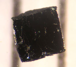
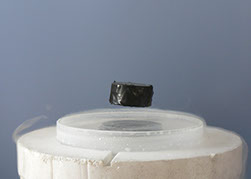
A small sample of the high-temperature superconductor BSCCO-2223.
Standard Materials
YBCO(Y1Ba2Cu3Ox),
LaBaCuO,
NdBaCuO,
PrBaCuO,
SmBaCuO,
BSCCO,
BKBO,
Nd2CuO4,
Gd2CuO4.
High Temp. Superconduction
High-temperature superconductors (abbreviated high-Tc or HTS) are materials that behave as superconductors at unusually[1] high temperatures. The first high-Tc superconductor was discovered in 1986 by IBM researchers Georg Bednorz and K. Alex Müller,[2][3] who were awarded the 1987 Nobel Prize in Physics "for their important break-through in the discovery of superconductivity in ceramic materials".
Whereas "ordinary" or metallic superconductors usually have transition temperatures (temperatures below which they superconduct) below 30 K (−243.2 °C), HTS have been observed with transition temperatures as high as 138 K (−135 °C).[2] Until 2008, only certain compounds of copper and oxygen (so-called "cuprates") were believed to have HTS properties, and the term high-temperature superconductor was used interchangeably with cuprate superconductor for compounds such as bismuth strontium calcium copper oxide (BSCCO) and yttrium barium copper oxide (YBCO). However, several iron-based compounds (the iron pnictides) are now known to be superconducting at high temperatures
The Meissner effect or a magnet levitating above a superconductor (cooled by liquid nitrogen)
Standard Materials
(Reactive Nitride) AI,Ti,Ti-Al, Cr, Zr, Hf
(Lubricated) MoS2, C,
Hard Coating
Hard coatings for wear resistance are commonly used in the cutting tool industry. The application of such coatings can be performed by a number of methods:
Arc evaporation (e.g. Sulzer, Ionbond, Hauzer)
Thermal evaporation (electron beam) (e.g.Oerlikon Balzers, TecVac)
Magnetron sputtering (e.g. Cemecon, Hauzer, TCL)
Environmental and economic considerations have emphasized the trend for more dry machining. Advanced wear-resistant coatings with increased oxidation resistance such as PVD TiAlN offer an advantage for dry machining of cast iron and alloyed steel. Although some important cutting operations are still not possible without coolants, further possibilities for dry drilling and tapping of steels are enabled by the recent approach using tools with hard coating layers topped with a lubricant layer. The combination of hard/soft coating layers allows improved chip flow with a lowered coefficient of friction and reduced cutting force. In this work, the hard/soft coating consists of a low-internal-stress TiAlN (hard layer) and WC/C (lubricant layer) of medium microhardness and low coefficient of friction. Both coating types are produced economically and reproducibly in one production scale PVD coating system. Recent performance data from field tests will be presented.
Standard Materials
Li(La) CoO2,
Li(La) NiO2,
Li(Co,Ni)O2,
LiMn2O4,
YSZ
Battery Cell
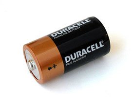
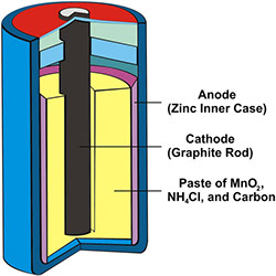
An electric battery is a device consisting of two or more electrochemical cells that convert stored chemical energy into electrical energy. Each cell contains a positive terminal, or cathode, and a negative terminal, or anode. Electrolytes allow ions to move between the electrodes and terminals, which allows current to flow out of the battery to perform work. Although the term battery technically means a device with multiple cells, single cells are also popularly called batteries.
.jpg?crc=479886827)
Standard Materials
Ni,
Cr,
Ni-Cr,
Ni-Cr-Fe,
Cu-Ni,
Cr-SiO,
Cr-Si,
Ta,Mo,
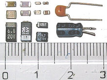
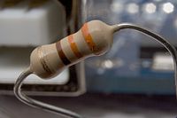
Resistor & Capacitor
A capacitor (originally known as a condenser) is a passive two-terminal electrical component used to store energy electrostatically in an electric field. The forms of practical capacitors vary widely, but all contain at least two electrical conductors (plates) separated by a dielectric (i.e. an insulator that can store energy by becoming polarized). The conductors can be thin films, foils or sintered beads of metal or conductive electrolyte, etc. The nonconducting dielectric acts to increase the capacitor's charge capacity. A dielectric can be glass, ceramic, plastic film, air, vacuum, paper, mica, oxide layer etc. Capacitors are widely used as parts of electrical circuits in many common electrical devices. Unlike a resistor, an ideal capacitor does not dissipate energy. Instead, a capacitor stores energy in the form of an electrostatic field between its plates.
A resistor is a passive two-terminal electrical component that implements electrical resistance as a circuit element. Resistors act to reduce current flow, and, at the same time, act to lower voltage levels within circuits. In electronic circuits, resistors are used to limit current flow, to adjust signal levels, bias active elements, and terminate transmission lines among other uses. High-power resistors that can dissipate many watts of electrical power as heat may be used as part of motor controls, in power distribution systems, or as test loads for generators. Fixed resistors have resistances that only change slightly with temperature, time or operating voltage. Variable resistors can be used to adjust circuit elements (such as a volume control or a lamp dimmer), or as sensing devices for heat, light, humidity, force, or chemical activity.
Standard Materials
AZO,
GZO,
ZnO,
SnO2,
ITO,
Si
SiAl,
Cr,
Ti,
Ni(V),
Al,
CuIn,
CuGa,
CIG,
Se
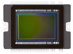
Sensor
A sensor is a transducer whose purpose is to sense (that is, to detect) some characteristic of its environments. It detects events or changes in quantities and provides a corresponding output, generally as an electrical or optical signal; for example, a thermo couple converts temperature to an output voltage. But a mercury-in-glass thermometer is also a sensor; it converts the measured temperature into expansion and contraction of a liquid which can be read on a calibrated glass tube.
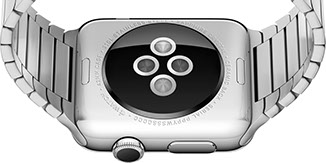
The heart rate sensor can also use infrared light. This mode is what Apple Watch uses when it measures your heart rate every 10 minutes.
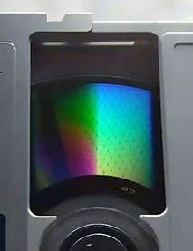
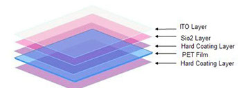
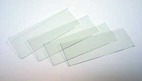
ITO Glass
Flat Glass
On the surface of the common glass coated with a layer of indium tin oxide conductive film, to form the indium tin oxide glass which common used in LCD, usually referred to as ITO glass.
ITO as nanometer indium tin oxide, has good conductivity and transparency, can cut off the harmful electromagnetic radiation, ultraviolet light and far infrared ray to human body. Therefore, after spraying in glass, plastic and electronic display screen, not only keep them to enhance conductivity and transparency and also to cut off harmful electronic radiation, ultraviolet and infrared to human body at the same time.
ITO conductive glass is on the basis of the calcium-sodium or borosilicate substrate, using the method of magnetron sputtering plating a layer of indium tin oxide (commonly known as ITO) film. Processing LCD special ITO conductive glass, before plating ITO layer, also plating a 20-30 nm thick layer of silicon dioxide as the barrier layer, the main effect is to prevent the metal ion in the calcium-sodium substrate diffusion penetration to the ITO layer, it will effect the conductivity of ITO layer. High-grade LCD special used ITO glass, in order to get a more uniform display control, before sputtering ITO layer, the substrate glass need to be polished.
The advanced ITO coating production line and mature management of processing technology, JMT can produce high and low resistance TN\STN of ITO conductive glass (the minimum 3 ohm ultra-low resistance ITO glass) and the ITO glass for touch screen, optical shadow elimination ITO glass, OGS monolithic (BM + ITO) coated glass, OGS large (BM+ ITO) coated glass, TFT low-temperature ITO coated glass etc.
Standard Materials
ITO,
AZO,
Ti(TixOy),
Cr,
NiCr,
Sn,
Ag
Display
Photo Mask
Semiconductor
Dielectric & Electrode
GMR Head
GMR For Laser Ablation
Hard Disks
Optical Magnetic Memory
Phase Change of Optical Memory
High Temp. Superconduction
Hard Coating
Battery Cell
Resistor & Capacitor
Sensor
Flat Glass
Our ISO 9001:2008 certified Materials Division stocks a vast assortment of pure materials, evaporation sources, and crucible liners for use in both thermal and E-beam evaporation as well as sputter deposition processes. We offer pure elements, compounds, alloys, ceramics, intermetallics, and mixtures in a variety of shapes, sizes, and purities for R&D applications. We also offer our materials customers sputter target bonding and precious metals reclamation services, saving you both time and money.
Contact sales@summit-tech.com.tw & for your custom R&D or production materials needs.
The Summit-Tech Company is an ISO:9001-2015 certified company. Copyright ©1996-2016 Summit-Tech Company® All rights reserved.